
- Insulators, conductors and semiconductors
- The function of a microchip
- The process to create a microchip
Age Levels: 10 – 14
Lesson Plan Presentation
Materials & Preparation
Build Materials
Materials and Preparation
- E-book
- Videos
- Playdoh – 5-6 small cans total per team
- Clay – 2-3 pieces per team
- 2-6 White LEDs (20mm- fun larger size)
- 6-10 White LEDs (5mm) – with legs trimmed shorter (make sure to keep polarity)
- (6V) AA battery holder with wires
- 4AA Batteries (could also use a 9V battery and clip with wires)
- Index Card (Cut into a circle about 3” in diameter. You can use the bottom of a cup)
- Sandwich Bag (cut in a circle slightly larger than 3” diameter)
- Pencil
- Tweezers
- Scissors
- Hole Punch
- Student worksheets
Testing Materials & Process
Materials
-
- Conductivity tester
- Testing items
Process
Teams use their conductivity tester to test each of their selected items by placing the item between the two metal fasteners. If the bulb lights up, the item conducts electricity. If the bulb does not light up, the item does not conduct electricity. Teams should document which items are conductors and which are insulators on their worksheets.
-
Engineering Design Challenge
Design Challenge
Design and create the “mask”needed for the creation of a microchip and then use the mask in creating a model of a microchip. Embark on three challenges that lead to the microchip model.
Criteria
- Watch videos
- Create a circuit with Play-Doh
Constraints
Use only the materials provided.
Activity Instructions & Procedures
- Watch the video to learn about what a semiconductor is, how it is made, and why it is so important!
- Introduce Challenges 1-3 to the students.
You are an Integrated Circuit (IC) Designer. An Integrated Circuit (IC) Designer is like a city planner, but instead of designing roads and buildings, they create super-small electronic parts that go inside gadgets like phones and computers. Their job is to figure out how to arrange tiny resistors, transistors, and capacitors on a chip so they work together. They use computer programs to create a map of where each part should go, ensuring that there are circuits connecting all the parts for electricity to flow. Without ICs, our electronic gadgets wouldn’t work!In order to prepare you for the design task, students need to learn about insulators and conductors by creating a circuit with Play-Doh.
Challenge 1: Electric Dough
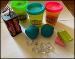
Materials Needed Per Team:- Play-Doh (conductor) – 3-5 small containers
- Clay (insulator)- 2-3 small pieces
- 2-6 White LEDs (20mm) per team
- (6V) AA battery holder with wire
- 4 AA batteries (or 9V battery and clip)
**See Teaching Tip Procedure - Students work in teams of two, but each individual creates a design to be tested.
- Hand out the student worksheets
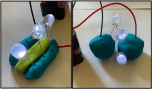
- Roll the conductive Play-Doh into two separate clumps. These will be the parts of the circuit that the electricity flows through. Make sure they’re close but not touching each other. Tip: if they touch that will short the circuit out.
- Insert the LED: LEDs have two legs: a longer one (positive) and a shorter one (negative). Push the longer leg into the clump connected to the positive side of the battery. Push the shorter leg into the other clump with the negative side.
- Complete the Circuit: When battery wires are inserted into the Play-Doh, the circuit is completed (or closed), allowing electricity to flow from the battery, through the Play-Doh, and light up the LED. **Teaching Tip: No need to use resistors. The playdoh IS the resistor. This is what makes squishy circuits, or Play-Doh work. Resistors would just make the LEDS super dim since the Play- Doh is so resistive.

- Play: Try creating different shapes with the conductive Play-Doh to see how it affects the circuit. Use the insulating Play-Doh to separate parts of the conductive Play-Doh if you want to make more complex circuits.
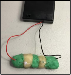
- Short Circuit: Remember, never let the two clumps of conductive Play-Doh touch directly, or you’ll create a short circuit.
- Series vs. Parallel Circuit: Note the images above are parallel circuits (all positive legs of the LEDs link and all negative legs of the LEDs link). Here is what it looks like in a series circuit (positive leg of one LED connected to the negative leg of another LED and so on).
- Chip Art: Before going to the next challenge read about Chip art
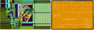
Electronic circuit scheme – orange background (vector illustration)
When engineers design integrated circuits, they use different shapes and boxes to make a plan, which is sometimes called ‘artwork.’ These shapes are like a secret code that tells the machines what to build. As we will learn, these boxes get converted into metals, insulators and semiconductors during manufacturing. But there are other kinds of art you can find on chips! Chip art, also known as silicon art, semiconductor art, silicon wafer art or chip graffiti refers to microscopic hidden doodles (designs, images, or messages) incorporated onto onto microchips during the manufacturing process. Engineers leave their creative mark on their tiny electronics canvases! One famous example was a hidden image of Waldo from the popular children’s book series, “Where’s Waldo?” that was found on the surface of a Texas Instruments silicon wafer in the late 1980s.

Source: https://www.devx.com/terms/chip-art/
To learn more about Chip Art watch this short video: Silicondoodle Medley by CPU Duke
Image Source: https://micro.magnet.fsu.edu/creatures/pages/waldo.html - Introduce Challenge 2
Students work in pairs but each student should try making their own mask. Team chooses one to use for the chip creation.
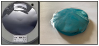
Challenge 2: Create the “Mask” which is a stencil of the circuit design. As the Integrated Circuit (IC) Designer, you need to create what is called a “mask.” The circuit design is turned into a mask (or stencil). During the challenge, you will then “stamp” your “mask” onto your wafer (making an imprint) transferring the circuit design onto your wafer. To make the mask, the circuit design is drawn (or stamped) onto the mask material and then cut out leaving the mask or stencil as the “negative of the circuit.” Light then transfers the circuit (imprinted) onto the wafer. In honor of the “Chip Art” we just learned about, we will turn our chip layout into art.
Two constraints:
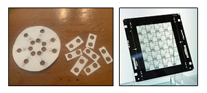
(1) must have a minimum of 6 “chips” (a single chip is two hole punches for the LED legs – see image of the six chips below)
(2) must have a recognizable image (our image is the “sun”). Consider these other samples (mountain and city skyline) or letters or numbers as well.Materials Needed:- Index Card** (Cut into a circle about 3” in diameter. You can use the bottom of a cup)
- Hole Punch
- Pencil
**A more high-tech option: If you have access to a 3D printer, you can design the “Mask” in the CAD program, Tinkercad, and then 3D print it.Procedure - Take the index card and cut out a 3”- 4” diameter circle as your maskMap out where to place 6-8 “chips” on your wafer. For this challenge, chips will contain a single LED, each which require two hole punches.
- You are the Quality Control Engineer or assign someone to this task. Explain that when quality control tests the chips they will close the circuit
 (using battery and wires) and if the LED lights up, it counts toward your yield. If you have 7 chips and 6 light up during testing, your yield will be 6 out of 7 or 86%. The goal is to have a yield of 100 %.
- Introduce Challenge 3
Again, students continue to work in teams of two, taking turns, alternating who does the steps.
Challenge 3: Take on the role of a Semiconductor Engineer working in a foundry or “Fab” (short for Fabrication Facilities) where you make microchips in a clean lab. Explore how a chip is made by making your own model with Play-Doh!While we don’t have a clean room here, we can learn what happens in “fab’ by using a few fun materials like Play-Doh – with some real semiconductors mixed in – to stand in for our silicon, masks and tools in the real fab.Materials Needed:- Play-Doh (3 small cans with different colors)

- Sandwich Bag
- Tweezers (optional)
- Batteries (4AA batteries)
- Battery holder (for 4AA batteries)
- LEDs (5mm) – with legs trimmed shorter (keeping
polarity- positive leg longer, negative leg shorter) - Scissors
- Hole Punch
 Step 1: Wafer. Silicon is mined and then made into an ingot. The ingot is sliced into thin “wafers.”
 Students Make: Begin with one layer of Play-Doh as the wafer.
Step 2: Clean & Polish. The wafer is cleaned and polished.
Students Make: Cut a sandwich bag to match the size of your wafer. Cover your wafer with it to show your wafer has been cleaned and polished.
Step 3: Photoresist Coating. After preparing the wafer, its surface is coated with a photoresist, a light-sensitive material.
Students Make: Add another layer of PlayDoh to model the photo resistant coating Step 4: Photo Mask. This Step has already been completed in Challenge #2 (making the mask)
Step 5: Etching. Etching is the process of removing unwanted material to create the features of the chip by using chemicals that eat away the wafer’s exposed areas, leaving behind the desired pattern. It also removes the underlying layers of silicon and other materials in the pattern of the circuit design.
Students Make: Place the mask on your wafer and use tweezers to remove the material exposed from your mask.
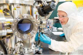
 Step 6: Deposition. Deposition involves adding a blanket of conducting or non-conducting materials depending on the desired properties of the final product. See the machine used to complete this step.
Students Make: Cut another circle (much larger than the wafer) from your sandwich bag. This will be a “blanket.” Cover your wafer with the blanket including all the areas etched away as the coating semiconducting materials. Use the tip of a LED to press the blanket to the holes (or areas that were etched). This pulls at the sandwich bag…work your way pressing the LED into the blanket and smoothing (one at a time).

Step 7: Vias. Vias are little wires that let us go from one layer to another – like an elevator for the circuit, we go from one layer to another ‘via’ the via!
Students Make: Place your vias as little pieces of playdoh to connect your layers. The top of each via is a ‘contact’ – where it will make contact to the next device.
Step 8: Doping: Doping is the process of changing the properties of silicon in the wafer to create different components of the chip. This is done by introducing impurities into the silicon, which changes its conductivity. The type and amount of impurities determine whether the silicon becomes n-type, which has an excess of electrons, or p-type, which has a shortage of electrons. These are made with big machines called ion implanters, and where n and p meet (a PN junction), makes the basis of a transistor!
Student Make: Light emitting diodes (LEDS) are actually just a PN junction, so since we don’t have a big implanter, we place our already made PN junctions (LEDS) from contact to contact to complete the circuit.
Step 9: Repeat. The photolithography, etching, and doping processes are repeated multiple times to build up the complex structures of the chip. Each repetition adds a new layer to the chip, with each layer serving a specific function in the final circuit.
 Step 10: Quality Control. Quality Control Engineers test the chips to ensure they will actually work. This technology can be delicate and even damage not visible to the human eye can hinder its function. Therefore, clean rooms are essential to keep out any impurities and maximize the number of chips a wafer creates.
Students Make: Carefully add your LEDs and then the QA Engineer will test each ”chip” using two wires and a battery to see if your LEDs light up.Step 11: Yield. Have students determine the yield. How many chips can you get out of your wafer? Typically a wafer with approximately a 12 inch diameter can yield 300-400 chips, depending on the amount of space between them.
Last Steps. Discuss these last steps that are needed to get the chip into your gadget
Packaging: Microchips need to be kept safe, just as you would protect a delicate sculpture with bubble wrap. This protection is provided by electronic packaging, which acts like this bubble wrap, safeguarding the chip from damage and ensuring it stays connected to the device’s main board, known as the printed circuit board (PCB).
- Assembly of chips into a gadget: Electronic assembly is akin to crafting an intricate puzzle. Each chip, once encased in its protective packaging, must find its precise place within the gadget, much like each puzzle piece fits into a specific spot. In factories, skilled workers or advanced robots position the chips accurately. After placement, these chips must communicate, achieved through delicate wires or soldering, akin to the puzzle pieces interlocking firmly.
- Testing: The final stage is rigorous testing, ensuring the gadget functions seamlessly, similar to the satisfying snap of the last puzzle piece fitting perfectly into place.
- Play-Doh (3 small cans with different colors)
Time Modification
The lesson can be done in as little as 1 class period for older students. However, to help students from feeling rushed and to ensure student success (especially for younger students), split the lesson into two periods giving students more time to brainstorm, test ideas and finalize their design. Conduct the testing and debrief in the next class period.
Engineering Design Process
Background Concepts
Read the ebook
Watch Videos
What is a Semiconductor?
 Let’s review from the video, what exactly a semiconductor is. Well first – what is a conductor? Well, it is something like a metal (like copper), that is good at conducting electricity. It is also an insulator – material that can’t conduct, like rubber. A semiconductor is a unique material that can be made to do both! Sometimes it conducts, sometimes it doesn’t. It can be used in things like computers and phones to make tiny switches called transistors.
Silicon is the most common semiconductor. It’s like the superhero of electronics! By adding different atoms to silicon, we can change its behavior. We create two types of semiconductors: n-type (which has extra electrons) and p-type (which has “holes” where electrons can move around). Other semiconductor materials are being used as well like germanium or compounds such as gallium arsenide. They are just right for creating electronic magic!
Why are Semiconductors Important?
They’re the building blocks of modern electronics! Think of transistors (tiny switches) that control everything in your computer, phone, and other gadgets. Without semiconductors, we wouldn’t have these amazing devices. So, remember: Semiconductors are like the “Goldilocks” of materials—they’re not too conductive, not too insulating, but just right for powering our tech!
Semiconductors are in almost everything now: computers, smartphones, cars, household appliances, gaming systems, and medical equipment. As a result, semiconductors are incredibly important for today’s economy, as they drive innovation and productivity in many industries.
What is the Semiconductor Supply Chain?
Supply chains are like intricate webs connecting factories, warehouses, trucks, ships, and stores. They ensure that products—whether it’s the latest smartphone, a trendy fashion item, or a beloved toy—reach us efficiently. But what happens when this delicate balance is disrupted?Let’s explore some common causes:
1. Natural Disasters: Mother Nature can be fierce. Earthquakes, hurricanes, floods, or wildfires wreak havoc on roads, factories, and shipping routes. Imagine a toy factory in a flood-hit area—production stalls, and toys can’t make their way to stores.
2. Transportation Delays: Trucks break down, ships get stuck in canals and planes face delays. These glitches ripple through the supply chain. If a crucial shipment of silicon chips for phones gets delayed, it affects phone production worldwide.
3. Global Demand Surges: Picture the latest gaming console hitting the market. Everyone wants it! But factories can only produce so many at once. When demand outpaces supply, shortages occur. Suddenly, getting your hands on that console becomes a quest.
4. Labor Shortages: Factories need skilled workers. If people fall sick or can’t work due to health crises (like the recent pandemic), production slows down. Fewer workers mean fewer toys, gadgets, and gizmos.
5. Geopolitical Tensions: Countries trade with each other, but sometimes politics gets in the way. Tariffs, trade disputes, or sanctions disrupt the smooth flow of goods. Imagine a toy made in Country A, assembled in Country B, and shipped to Country C—any tension between these nations affects the process.
6. Supplier Woes: A foundry relies on raw materials like silicon, gallium, gold and even iridium (even rarer than gold!). If a storm wipes out an iridium mine, the entire industry suffers. Suddenly, phones, game consoles, and electronic toys become scarce. The supply chain is only as strong as its weakest link.
7. Just-in-Time Inventory: Many companies keep minimal stock—they order just what they need when they need it. It’s efficient, but risky. If a single supplier falters, the whole chain stumbles. Imagine dominoes falling.
In the end, supply chains are complex systems, akin to a well-choreographed dance amidst chaos. Each disruption sends ripples that touch our lives. As you unbox a new gadget or toy, think of the intricate journey it took to reach you. It’s a testament to the steadfast dedication of those who maintain the flow of goods, despite the challenges of nature and circumstance.
Vocabulary
See (ebook for more)
- Conductor – material that allows electricity to pass through it, like a metal (copper, gold and silver for example).
- Insulator – material that doesn’t allow electricity to pass through it, like rubber, glass and plastic for example.
- Semiconductor – is a special material that is both conductor and insulator of electricity! Sometimes it conducts, sometimes doesn’t. Silicon and gallium are examples of semiconductor materials.
- Ingot – Silicon is mined and then made into an ingot. Silicon is melted, tiny amounts of other elements are added to make it a particular type of silicon. A rod is dipped into the molten silicon and when it is pulled out the silicon cools and solidifies making the shiny cylindrical stick of silicon. The ingot is then sliced into thin “wafers”
- Wafer – is a thin slice of semiconductor material used to make microchips that is cut from an Ingot.
- Microchip (also known as: semiconductor chip, semi, and chip) – is an integrated circuit (IC) that is etched on the wafers.
- Integrated circuit (or microchip) is a small computer containing tiny switches that perform arithmetic and logic operations and provide temporary memory storage.
- Transistor – is a tiny switch that can amplify or control electrical signals. It performs arithmetic and logic operations and provides temporary memory storage.
- Nanoscale – is incredibly small – a billion times smaller than what we can see with our eyes. (For example, chips are made on a nanoscale). There are billions of transistors on a microchip.
- Moore’s Law is like a growth spurt for computers! Gordon Moore, the co-founder of Fairchild Semiconductor and Intel, predicted, in 1975, that the number of transistors (tiny switches) on a microchip would double about every two years.
- Foundry or “Fab” (short for Fabrication Facilities) – where you make microchips.
- Clean Lab – in a clean lab, everything is ultra-clean. Even a speck of dust can mess up the chips! That speck of dust can interfere with the conductive network on a chip. It’s a high-tech space where cleanliness is king!
- Resistance: Insulation is measured in resistance. The more insulating a material, the more resistance it has
- Parallel Circuit: Allows multiple paths for electricity (current) to flow through
- Series Circuit: Allows one path for electricity (current) to flow through
Manufacturing Process of Making a Microchip:
- Clean & Polish – the wafer is cleaned and polished.
- Photoresist Coating – after preparing the wafer, its surface is coated with a photoresist, a light-sensitive material as part of the “photolithography” process.
- Photo Mask – the circuit design is turned into a mask (or stencil). To make the mask, the circuit design is drawn (or stamped) on the mask material and then and then cut out leaving the mask or stencil of the “negative of the circuit.” Light then transfers the circuit (imprinted) onto the wafer, exposing the parts that should be removed in the next step. We call this step of making the mask, the ‘tapeout’ since masks used to be made with tape.
- Etching – the process of removing unwanted material to create the features of the chip by using chemicals that eat away the wafer’s exposed areas, leaving behind the desired pattern. It also removes the underlying layers of silicon and other materials in the pattern of the circuit design.
- Deposition – involves adding a blanket of conducting or non-conducting materials depending on the desired properties of the final product.
- Doping – the process of changing the properties of silicon in the wafer to create different components of the chip. This is done by introducing impurities into the silicon, which changes its conductivity. The type and amount of impurities determine whether the silicon becomes n-type, which has an excess of electrons, or p-type, which has a shortage of electrons. These are made with big machines called ion implanters, and where n and p meet (a PN junction), makes the basis of a transistor!
- Vias – are little wires that let us go from one layer to another – like an elevator for the circuit, we go from one layer to another ‘via’ the via!
- Quality Control – Quality Control Engineers test the chips to ensure they will actually work. This technology can be delicate and even damage not visible to the human eye can hinder its function. Therefore, clean rooms are essential to keep out any impurities and maximize the number of chips a wafer creates.
Chip Art – is also known as silicon art, semiconductor art, silicon wafer art or chip graffiti refers to microscopic hidden doodles (designs, images, or messages) incorporated onto microchips during the manufacturing process.
Supply Chain – is an intricate web connecting factories, warehouses, trucks, ships, and stores. They ensure that products reach us efficiently.
Short Circuit – is when wires that are not supposed to come in contact with each other touch (overlap in someway).
Parallel Circuit – allows multiple paths for electricity (current) to flow through.
Series Circuit – allows one path for electricity (current) to flow through.
Resistance – in electrical circuits, resistance is like a “crowd” that makes it tougher for electric charges (like tiny electrons) to move around. Insulators have resistance and the more insulating a material, the more resistance it has.
PN Junction – is a special region where two types of semiconductor materials come together in a single crystal. P-Type Semiconductor (p-side): This part contains electron holes (which are like missing electrons). It’s called “p-type” because it has a positive charge. N-Type Semiconductor (n-side): This part contains freely-moving electrons. It’s called “n-type” because it has a negative charge. P-N Junction: The boundary where the p-type and n-type materials meet is called the p-n junction. It’s like a barrier between the two regions.
Dig Deeper
Semiconductor Missions – See full mission descriptions
Welcome! Join us on this grand mission (made up of several smaller missions) as we learn more about the world of semiconductors. There are five missions to explore. They will challenge you to dig deeper into understanding semiconductors, semiconductor technology, supply chain and its impact on our world.
Mission (1) – Materials MIssion: Superhero of Electronics
- Insulator & Conductor PhET Simulation
- Semiconductors Types PhET Simulation
Mission (2) – Design Mission: Art Infusion (This Lesson)
- Integrated Circuit Designer Certification -“Squishy Circuit”
- Create the “Mask”
Mission (3) – Nanoscale Mission: Moore’s Law
- Graphing Moore’s Law
- Predicting the Future
Mission (4) – History Mission: Transistor Revolution
- Debate on significance of transistor
Mission (5) – Supply Chain Mission: Science Fiction Saga
- Supply chain disruption team story
Global Functional Alignment
Alignment to Curriculum Frameworks
The “Notes” column explains how the lesson connects to STEM topics and a “X” indicates at what level (beginner, intermediate, advanced). Please note a large “X” indicates a strong connection and a small “x” indicates a weaker connection or opportunity to make a connection.
Science Lesson Alignment Beginner Intermediate Advanced Materials & Properties Conductor, Insulator, Semiconductor x Technology & Engineering Lesson Alignment Beginner Intermediate Advanced Information Technology Microchip Technology X Systems Microchip Manufacturing, Supply Chain X Design & Innovation Design a Mask for the Microchip Process
Construct a model of a MicrochipX Related Engineering Fields and Degrees
Careers in Semiconductor Industry
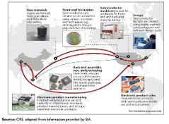
 As you saw in the video, there are so many diverse careers in the semiconductor industry! Review the graphic of semiconductor careers and engineering disciplines. Many engineers have the skills and knowledge to perform multiple functions.
 Student Worksheet
Student Worksheet – Three Challenges
- Challenge 1: Squishy Circuits
- Challenge 2: Create the Mask
- Challenge 3: Make the Chip
Challenge 1: Squishy Circuits
You are an Integrated Circuit (IC) Designer. An Integrated Circuit (IC) Designer is like a city planner, but instead of designing roads and buildings, they create super-small electronic parts that go inside gadgets like phones and computers. Their job is to figure out how to arrange tiny resistors, transistors, and capacitors on a chip so they work together. They use computer programs to create a map of where each part should go, ensuring that there are circuits connecting all the parts for electricity to flow. Without ICs, our electronic gadgets wouldn’t work!
In order to prepare you for the design task you need to learn about insulators and conductors by creating a circuit with Play-Doh.Materials Needed:
- Playdoh (conductor)
- Clay (insulator)
- 2-6 White LEDs (20mm)
- 9V Battery and clip (or AA battery holder with wires 4AA (6V)
Procedure
 Roll the conductive Play-Doh into two separate clumps. These will be the parts of your circuit that the electricity flows through. Make sure they’re close but not touching each other. Tip: if they touch that will short the circuit. Use the clay (insulator) to keep the conductive material from touching and shorting the circuit.
 Insert the LED: LEDs have two legs: a longer one (positive) and a shorter one (negative). Push the longer leg into the clump connected to the positive side of the battery. Push the shorter leg into the other clump with the negative side.
- Complete the Circuit: When you insert the battery wires into the Play-Doh (make sure you have considered polarity), you complete the circuit (or close the circuit), allowing electricity to flow from the battery, through the Play-Doh, and light up the LEDs.
- Play: Try creating different shapes with your conductive Play-Doh to see how it affects the circuit. Use the insulating Play-Doh to separate parts of the conductive Play-Doh if you want to make more complex circuits.
Challenge 2: Create the “Mask”
A mask is a stencil of the circuit design. As the Integrated Circuit (IC) Designer, you need to create what is called a “Mask.” The circuit design is turned into a mask (or stencil). During the challenge, you will then “stamp” your mask onto your wafer (making an imprint) transferring the circuit design onto your wafer. To make the mask, the circuit design is drawn (or stamped) on the mask material and then cut out leaving the mask or stencil of the “negative of the circuit.” Light then transfers the circuit (imprinted) onto the wafer.
Chip Art: Before getting started on this next challenge read about Chip Art
When engineers design integrated circuits, they use different shapes to make a plan. This plan is sometimes referred to as ‘artwork,’ but it’s not the kind you hang on the wall. It’s a blueprint for something amazing. These shapes are like a secret code that tells the machines what to build. As we will learn, these shapes get converted into metals, insulators and semiconductors during manufacturing. But there are other kinds of art you can find on chips! Chip art, also known as silicon art, semiconductor art, silicon wafer art or chip graffiti refers to microscopic hidden doodles (designs, images, or messages) incorporated onto microchips during the manufacturing process. Engineers leave their creative mark on their tiny electronics canvases! One famous example was a hidden image of Waldo from the popular children’s book series, “Where’s Waldo?” that was found on the surface of a Texas Instruments silicon wafer in the late 1980s.
 Source: https://www.devx.com/terms/chip-art/
Go deeper by watching : To learn more about Chip Art watch this short video: Silicondoodle Medley by CPU Duke Image Source: https://micro.magnet.fsu.edu/creatures/pages/waldo.htm
In honor of the “Chip Art” we just learned about. We will turn our chip layout into art.
Two constraints:
(1) must have a minimum of 6 “chips” (A single chip is two hole punches for the LED legs – see image of the six chips below)
(2) must have a recognizable image (see image is the “sun”). Consider these other samples (mountain and city skyline) or letters and numbers as well.
Material
- Index Card** (Cut into a circle about 3” in diameter. You can use the bottom of a cup)
- Hole Punch
- Pencil
**A more high-tech option: If you have access to a 3D printer, you can design the “Mask” in the CAD program, Tinkercad, and then 3D print it.
Procedure- Take the index card (cut out a 4” diameter circle as your wafer) and map out where to place 6-8 “chips” on your wafer. For this mission, chips will contain a single LED.
- There is a twist. In honor of the “Chip Art” we just learned about. We will turn our chip layout into art. Two constraints: (1) must have a minimum of 6 “chips” (2) must have a recognizable image (see image is the “sun”). Consider these other samples (mountain and city skyline) or letters and numbers as well.
- You are the quality control engineer or assign someone to this task. Explain that when quality control tests the chips they will close the circuit (using battery and wires) and if the LED lights up it counts toward your yield. If you have 7 chips and 6 light up during testing your yield will be 6 out of 7 or 86%. The goal is to have a yield of 100.
Challenge 3: Making a Chip
Take on the role of semiconductor engineers working in a foundry or “Fab” (short for Fabrication Facilities) where you make microchips in a clean lab. Explore how a chip is made by making your own model with PlayDoh!
While we don’t have a clean room here, we can learn what happens in a ‘fab’ by using a few fun materials like PlayDoh – with some real semiconductors mixed in – to stand in for our silicon, masks and tools in the real fab.
Materials Needed:
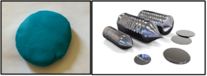
- PlayDoh (3 cans with different colors)
- Sandwich Bag
- Tweezers
- Batteries (4AA batteries)
- Battery holder (for 4AA batteries)
- LEDs (5mm) – with legs trimmed shorter
- Scissors
- Step 1: Wafer. Silicon is mined and then made into an ingot. The ingot is sliced into thin “wafers”
Students Make: Begin with one layer of PlayDoh as the wafer.
 Step 2: Clean & Polish. The wafer is cleaned and polished.
Students Make: Cut a sandwich bag to match the size of your wafer. Cover your wafer with it to show your wafer has been cleaned and polished.

- Step 3: Photoresist Coating. After preparing the wafer, its surface is coated with a photoresist, a light-sensitive material.
Students Make: Add another layer of PlayDoh to model the photo resistant coating
- Step 4: Photo Mask. (if you completed challenge #2 you already did this step!) The circuit design is turned into a mask (or stencil). To make the mask, the circuit design is drawn (or stamped) on the mask material and then and then cut out leaving the mask or stencil of the “negative of the circuit.” Light then transfers the circuit (imprinted) onto the wafer,exposing the parts that should be removed in the next step. We call this step of making the mask ‘tapeout’ since masks used to be made with tape.
Students Make: Take the index card (cut out a 4” diameter circle as your wafer) and map out where to place 6-8 “chips” on your wafer. For this mission, chips will contain a single LED. There is a twist. In honor of the “Chip Art” we just learned about. We will turn our chip layout into art. Two constraints: (1) must have a minimum of 6 “chips” (2) must have a recognizable image (see image is the “sun”). Consider these other samples (mountain and city skyline). When quality control tests your chips they will close the circuit (using battery and wires) and if it lights up it counts toward your yield! If you have 7 chips and 6 light up during testing your yield will be 6 out of 7 or 86%. The goal is to have a yield of 100%. - Step 5: Etching. Etching is the process of removing unwanted material to create the features of the chip by using chemicals that eat away the wafer’s exposed areas, leaving behind the desired pattern. It also removes the underlying layers of silicon and other materials in the pattern of the circuit design.
Students Make: Use tweezers to remove the material exposed from your mask.
 Step 6: Deposition. Deposition involves adding a blanket of conducting or non-conducting materials depending on the desired properties of the final product. See the machine used to complete this step.
Students Make: Cut another circle (much larger than the wafer from your sandwich bag and cover your wafer including all the areas etched away to as the coating semiconducting materials. Use the tip of a LED to press the blanket to the holes (or areas that were etched). This pulls at the sandwich bag…work your way pressing LED into blanket and smoothing (one at a time)
Step 7: Vias. Vias are little wires that let us go from one layer to another – like an elevator for the circuit, we go from one layer to another ‘via’ the via! , via Wikimedia Commons” v:shapes=”image3.jpg”>
 Students Make : Place your vias as little pieces of playdoh to connect your layers. The top of each via is a ‘contact’ where we will make contact to the next device.
 Step 8: Doping. is the process of changing the properties of silicon in the wafer to create different components of the chip. This is done by introducing impurities into the silicon, which changes its conductivity. The type and amount of impurities determine whether the silicon becomes n-type, which has an excess of electrons, or p-type, which has a shortage of electrons. These are made with big machines called ion implanters, and where n and p meet (a PN junction), makes the basis of a transistor!
Students Make: Light emitting diodes (LEDS) are actually just a PN junction, so since we don’t have a big implanter, we place our already made PN junctions (LEDS) from contact to contact to complete the circuit.
 Step 9: Repeat. The photolithography, etching, and doping processes are repeated multiple times to build up the complex structures of the chip. Each repetition adds a new layer to the chip, with each layer serving a specific function in the final circuit.
Students Make: Imagine you have repeated these steps to make multiple layers.
- Step 10: Quality Control. Quality Control Engineers test the chips to ensure they will actually work. This technology can be delicate and even damage not visible to the human eye can hinder its function. Therefore, clean rooms are essential to keep out any impurities and maximize the number of chips a wafer creates.
Students Make: Carefully add your LEDs and then the QA Engineer will test each ”chip” using two wires and a battery to see if your LEDs light up.
- Step 11: Yield. Have students determine the yield. How many chips can you get out of your wafer? Typically a wafer with approximately a 12 inch diameter can yield 300-400 chips, depending on the amount of space between them.
Semiconductor Resources
Videos
- Introduction to semiconductors with Kathy Hayashi webinar by IEEE USA
- Chips Are Difficult to Make, and It’s Even Harder During a Supply Crunch by WallStreet Journal
- “ChipIn” video series by RoadTrip Nation and hosted by Semi Foundation
- From Sand to Silicon: The Making of a Chip by Intel
- Samsung Semiconductor Newsroom – YouTube by Samsung
- How are Microchips Made? By Interesting Engineering
- Zoom into a Microchip video by NISENet
- Transistors: Teeny Tech that Changed the World by Abby Kent (Project for Science and Natural History Filmmaking from Montana State University)
- Transistors – The Invention That Changed The World by Real Engineering
- Silicondoodle Medley by CPU Duke
Simulations
- UC Davis Semiconductor Manufacturing Training
- Phet Semiconductor Simulation
- Every Circuit
- Wokwi
- Tinkercad Circuits
- vFabLab is a virtual clean room by Purdue University and Intel
Design and Print a Chip
- Tiny Tapeout
- Efabless
- Patchr (PCB Design)
Other Lessons on Semiconductors
- Semi Foundation hosts semiconductor resources for teachers
- Semiconductor Resources for all grade levels by Ignited
- Semiconductor Introduction featuring Glossary by Computer History
- Semiconductor Diodes Lesson by Nagwa
Encyclopedias & Glossary
- PCMag Encyclopedia by PCMagazine
- Computer History Glossary by Computer History Museum
- Britannica Kids by Encyclopedia Britannica
- Semiconductor Facts for Kids by Kids Encyclopedia Facts
- Periodic Table of Elements by Minerals Education Coalition.
Articles or Guides
- An Introductory Guide to Semiconductors by RS Components
- Common Misconceptions About Printed Circuit Board Design by Arlington Cardinal
- The Main Types of Chips Produced by Semiconductor Companies by Investopedia
- The Ultimate Guide to Semiconductor Packaging by anysilicon
- Semiconductors: What Is the Supply Chain? Why Is it Important? By Investopedia
- Mapping the Semiconductor Supply Chain: The Critical Role of the Indo-Pacific Region by Center for Strategic & International Studies
- Where is Waldo Chip Art by National High Magnetic Field Laboratory
- Silicon Earth: A Historical Perspective on the Invention/Discovery of the Transistor by John Cressler
- Results from Semiconductor Supply Chain Request for Information by US Department of Commerce
Translations