
Nanotechnology

TRYENGINEERING CAREER PATHWAYS
Nanotechnology
Nanotechnology is science, engineering, and technology conducted at the nanoscale, which is about 1 to 100 nanometers. Nanoscience and nanotechnology are the study and application of extremely small things and can be used across all the other science fields, such as chemistry, biology, physics, materials science, and engineering.
Most industries have been impacted by work done at the nanoscale. And, while many of these applications are still in various stages of research, many products and techniques have impacted everything from clothing, to medicine delivery, to diagnostics, to energy and are commercially available.
What makes it unique?
This field is in a high growth stage, where researchers are applying nanotechnology to applications in many industries. Those working with nanotechnology find it invigorating to develop applications and see they come to fruition to make an impact on the world.
 Degree Connections
The following are examples of some accredited degrees leading to a career in nanotechnology:
- Nanotechnology
- Nanotechnology Engineering Technology
- Materials Engineering
- Bioengineering
- Electrical Engineering
- Chemical Engineering
Search our global database of accredited engineering programs.
Want to learn more?
Click on the blue tabs to explore the field in more detail and learn about preparation and employment, the green tabs to be inspired by people working at the nano scale and how they impact the world, and the orange tabs for ideas on how to learn more and you can get involved with activities, camps, and competitions!
Explore

Those working in nanotechnology work in offices or laboratories where they conduct research – or they may work for a medical product company and guide new products which incorporate nanotechnology. Those with nanotechnology degrees will often work in teams with others from other engineering specialties such as chemical, electrical, or others on a shared project. They might find themselves traveling to different work settings such as hospitals or manufacturing centers, depending on their focus area.
Their projects will focus on changing products and services by working at the nano level. So there is always a new project on the horizon.
An average work week is generally 40 hours in this field, with extra time needed if there is a deadline or a new product or service launch.
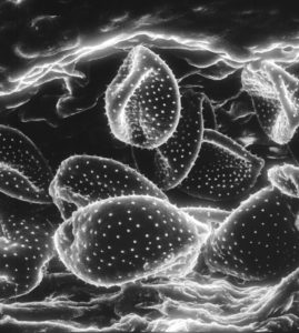
The Scanning Electron Microscope
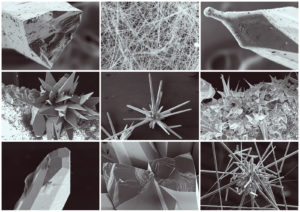
The electron microscope is integral to characterization of materials. Tens of thousands are in use globally because they have opened a world to materials at a very small scale. Iowa State University offers an explanatory website showing how the SEM works. Basically, a beam of electrons is focused upon a specimen, and an image and data is generated from electrons transmitted through the specimen that provide insight into its properties.
As an early example, in 1967, a Stereoscan Mark VI scanning electron microscope (SEM) was ordered by NASA’s Jet Propulsion Laboratory. Because they were new and in high demand, JPL had to wait nearly a year before it arrived. It was used by their electronic parts engineering section failure analysis laboratory to examine microcircuits for defects.
SEMs are used in medicine to compare samples of healthy and unhealthy tissues, or to observe the effect of medicine in treating disease. They are used in forensics to compare paint, inks, and hair samples involved in a crime. They are used to examine metals and other materials to look for flaws or for changes resulting from stress or chemicals.
Most famously, the Ford Motor Company instituted and promoted their assembly line for manufacturing automobiles which included a moving conveyor to speed production. Their assembly line, in 1913, reduced production time for a Model T Ford to 93 minutes and divided the work into 45 steps. They say that they could produce a car faster than the paint on the car could dry!
Find out more:

Nanotechnology research and development results in the development of new nanotechnology processes or in
prototypes of new or altered materials and/or products that may be used by various industries – from medical to materials to electronics. Automobile and aerospace firms are working with nanotechnology to improve surfaces and strength. In medicine, nano processes are used to help deliver drugs to targeted cancers.
The following is just a sample of some companies, in addition to government agencies, which employ those working in nanotechnology:
- Airbus Group
- Bausch & Lomb
- Beechcraft
- Boeing
- Boston Scientific
- Cessna
- Dassault Aviation
- Fillauer
- Ford Motor Company
- GE Healthcare
- General Motors
- GNF Systems
- Hershey’s
- Hitachi Healthcare
- Hologic
- INovio
- Intel
- Lucent Medical
- Medtronic
- Northrop Grumman
- Ortho EuropePiaggio
- SpaceX
- Texas Instruments
- Virgin Galactic

For most engineering careers:
- a bachelor’s degree is required
- a master’s degree may be recommended for those specializing or interested in management
- students may also start with a related associate degree and then move on to a bachelor’s when they have settled on a degree path.
- many students are required to participate in a co-op program while at university to gain real world experience in their chosen field.
- education doesn’t really stop…engineers need to stay current as technology changes and materials and processes improve over time.
- many professional societies offer certificates and coursework to support continuing education for their members.
At the undergraduate level, examples of courses in nanotechnology may focus on biomedical nanotechnology, nanotechnologies for energy and the environment, or other areas. Basic courses will include physical properties of materials, crystallography, electronic devices and circuits for nanoengineers, multiscale transport, and probability and statistics. Degrees specifically focused on nanotechnology are new in the past decade. You may also enter this field with an undergraduate degree in another area of science or engineering and then pursue a masters or PhD in nanotechnology.
It is important to select an engineering or nanotechnology degree that has been accredited to meet basic standards. Find out more and browse TryEngineering’s global database of accredited engineering and computing programs.
Be Inspired
One of the best ways to explore what it might be like to work in nanotechnology is to learn about people who contributed historically or are currently working in the field.
- Max Knoll was a German electrical engineer, who along with his co-worker, Ernst Ruska, invented the electron microscope in 1931.
- TryNano.org provides profiles of many professionals working in nanotechnology. A few examples include:
- John Yeow is the University Research Chair at the University of Waterloo in Canada whose research is devoted to understanding, modelling, designing, integrating, and developing micro/nanodevices for medical and industrial applications.
- Chennupati Jagadish is a Distinguished Professor at the Australian National University working on compound semiconductor nanostructures for optoelectronics, energy and neuroscience applications. His advice to students? “Choose something you are passionate about, dream big, aim high, learn as many skills as possible, and believe in yourself!” In the video to the right he explains his background and holographic phones!
- Herbert Bennett is a National Institute of Standards and Technology Fellow and Executive Advisor of NIST’s Semiconductor and Dimensional Metrology Division. He has worked for many years in theoretical solid-state physics, measurements for the performance of electronics, magnetic, and optical materials and devices, and development of international standards for such materials and devices.

Nanomedicine is the application of nanotechnology to traditional medicine and includes many examples that have already impacted our world. As this is a new area, we anticipate further positive impacts on medicine as researchers develop new ways to apply nanotechnology to drug delivery and treatment of disease.
As an example, chemotherapy for cancer treatments traditionally exposes many healthy parts of the body to the treatment. Using nanotechnology, chemotherapy can be targeted directly to a tumor and minimize exposure to the rest of the body.
As another example, the current treatment for advanced age-related macular degeneration requires monthly injections into the eye. But if instead the medication is slowly released from the inside of a nanoparticle, the patient might only need an injection twice a year.
Nanotechnology is also emerging as an exciting and promising new means of treating neurological diseases, colorectal cancer, and inflammatory bowel disease. While all are in research stages, nanomedicine is showing how looking at something small can have a bit impact on the world!
Find out more:
- Explore more details and applications at the Center for Nanomedicine at Johns Hopkins University.
- ASME: 10 Ways Nanotechnology Impacts our Lives
- Carbon nanotube “stitches” strengthen composites
- A new approach to making airplane parts, minus the massive infrastructure
Get Involved
Dig deeper into topics related to nanotechnology that interest you!

Explore:
- TryNano.org
- National Nanotechnology Initiative
- NASA Ames Research Center
- NanoHUB
- TryEngineering News Blog
Watch:
Try it Out:
- Explore an online Scanning Electron Microscope!
- Play some games that involve nanotechnology (placeholder):
- Try one of the TryEngineering lessons that focus on nanotechnology:

Clubs, competitions, and camps are some of the best ways to explore a career path and put your skills to the test in a friendly-competitive environment.
Clubs:
- Many schools have chemistry or electronic clubs or opportunities for students to get together and work on challenges that provide a good basis for any engineering degree.
Competitions:
- EnvisioNano Contest is a contest for undergraduate and graduate students conducting nanotechnology research.
- Nano Film is a video contest for undergraduate and graduate students that are conducting nanotechnology research
- Gennano is a competition asks middle and high school students to use scientific research to drive or equip an original superhero. Students can envision science that is grounded in current research but not yet possible, allowing them to learn about the potentials and limitations of real-world science and technology.
- International Nanotechnology Olympiad is an annual competition among university students to propose ideas and plans for nanotechnology based solutions to global challenges/
Camps:
- TryEngineering Summer Institute, US: Attend the TryEngineering Summer Institute to further your core engineering skills.
- NISENET High School Nanotechnology Summer Camp Framework
- UCLA Nanoscience Lab Summer Institute
- European School on Nanosciences and Nanotechnologies
- Many universities offer summer engineering experiences. Reach out to your local university’s engineering department to see what they offer.
Did you know you can explore nanotechnology in your community? While scanning electron microscopes are not generally available at your local school, try out a virtual one! Visit http://myscope-explore.org/virtualSEM.html and explore the tutorial and consider the following:
- Why does air need to be removed?
- What does accelerating voltage impact the final image?
- What does spot size focus on?
- Why would the height of the sample impact final image resolution?
- What samples do you think would be interestig to vie on an SEM? What would you be looking for?
- What medical applications can you think of for using a SEM? What would a doctor want to see an image of? What sort of image do you think a doctor might have had access to prior to SEM technology? What impact might that have had on a diagnosis or treatment?
Find out more:

Be sure to reach out to professional societies focused on nanotechnology where you live. Not all will offer membership to pre-university students, but most offer groups for university students, and certainly offer online resources to help you explore the field.
Some examples of groups focusing on nanotechnology:
Some resources on this page are provided or adapted from the US Bureau of Labor Statistics and the Career Cornerstone Center.